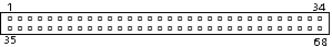
 68 pin MALE connector at the controller | CardBus, the 32-bit high performance bus mastering architecture for PC Cards, was standardized by the PCMCIA in May 1996. This bus is targeted to mobile computers. PCI-like 32-bit interface operates at a power-saving 3.3 volts, and cards can include standardized power-management mechanisms. The CardBus interface allows an I/O adapter or a memory module to be added to or removed without disrupting the system"s operation. It adds high bandwidth PCI-based capabilities to the PC Card technology.
CardBus PC Cards are attached to their host system through a sturdy 68-pin connector, which is common to all PC Cards. (CardBus cards employ a shielding shroud around this connector, to enhance their signal integrity).
CardBus cards adopt the well-established PC Card form-factors. There are different types of CardBus cards (sizes are TxLxW): - Type I: 3.3mm x 85.6mm x 54.0mm
- Type II: 5.0mm x 85.6mm x 54.0mm
- Type III: 10.5mm x 85.6mm x 54.0mm
CardBus provides a 32-bit multiplexed address/data path, which operates at PCI local-bus speeds of up to 33 MHz, yielding a peak bandwidth of 132MB/sec. CardBus accomplishes this by adopting the synchronous burst-transfer orientation of PCI, as well as a bus protocol, which is essentially identical to that of PCI.
|
Pin
|
Name
|
Description |
|
1 |
GND
|
Ground
|
|
2 |
CAD0
|
Address/Data 0 |
|
3 |
CAD1
|
Address/Data 1 |
|
4 |
CAD3
|
Address/Data 3 |
|
5 |
CAD5
|
Address/Data 5 |
|
6 |
CAD7
|
Address/Data 7 |
|
7 |
CCBE0#
|
Command/Byte Enable 0 |
|
8 |
CAD9
|
Address/Data 9 |
|
9 |
CAD11
|
Address/Data 11
|
|
10
|
CAD12
|
Address/Data 12
|
|
11
|
CAD14
|
Address/Data 14
|
|
12
|
CCBE1#
|
Command/Byte Enable 1 |
|
13
|
CPAR
|
Parity
|
|
14
|
CPERR#
|
Parity error
|
|
15
|
CGNT#
|
Grant
|
|
16
|
CINT#
|
Interrupt
|
|
17
|
Vcc
|
Vcc
|
|
18
|
Vpp1
|
Vpp1
|
|
19
|
CCLK
|
CCLK
|
|
20
|
CIRDY#
|
Initiator Ready
|
|
21
|
CCBE2#
|
Command/Byte Enable 2 |
|
22
|
CAD18
|
Address/Data 18
|
|
23
|
CAD20
|
Address/Data 20
|
|
24
|
CAD21
|
Address/Data 21
|
|
25
|
CAD22
|
Address/Data 22
|
|
26
|
CAD23
|
Address/Data 23
|
|
27
|
CAD24
|
Address/Data 24
|
|
28
|
CAD25
|
Address/Data 25
|
|
29
|
CAD26
|
Address/Data 26
|
|
30
|
CAD27
|
Address/Data 27
|
|
31
|
CAD29
|
Address/Data 29
|
|
32
|
RSRVD
|
Reserved
|
|
33
|
CCLKRUN#
|
CCLKRUN#
|
|
34
|
GND
|
Ground
|
|
35
|
GND
|
Ground
|
|
36
|
CCD1#
|
Card Detect 1 |
|
37
|
CAD2
|
Address/Data 2 |
|
38
|
CAD4
|
Address/Data 4 |
|
39
|
CAD6
|
Address/Data 6 |
|
40
|
RSRVD
|
Reserved
|
|
41
|
CAD8
|
Address/Data 8 |
|
42
|
CAD10
|
Address/Data 10
|
|
43
|
CVS1
|
|
|
44
|
CAD13
|
Address/Data 13
|
|
45
|
CAD15
|
Address/Data 15
|
|
46
|
CAD16
|
Address/Data 16
|
|
47
|
RSRVD
|
Reserved
|
|
48
|
CBLOCK#
|
Block ???
|
|
49
|
CSTOP#
|
Stop transfer cycle
|
|
50
|
CDEVSEL#
|
Device Select
|
|
51
|
Vcc
|
Vcc
|
|
52
|
Vpp2
|
Vpp2
|
|
53
|
CTRDY#
|
Target Ready
|
|
54
|
CFRAME#
|
Address or Data phase
|
|
55
|
CAD17
|
Address/Data 17
|
|
56
|
CAD19
|
CAD19
|
|
57
|
CVS2
|
|
|
58
|
CRST#
|
Reset
|
|
59
|
CSERR#
|
System Error
|
|
60
|
CREQ#
|
Request ???
|
|
61
|
CCBE3#
|
Command/Byte Enable 3 |
|
62
|
CAUDIO
|
Audio ???
|
|
63
|
CSTSCHG
|
|
|
64
|
CAD28
|
Address/Data 28
|
|
65
|
CAD30
|
Address/Data 30
|
|
66
|
CAD31
|
Address/Data 31
|
|
67
|
CCD2#
|
Card Detect 2 |
|
68
|
GND
|
Ground
|
Another representation (looking into card)
| |
|
|
|
|
|
| GND |
|
1 |
35 |
|
GND |
| CAD0 |
<-> |
2 |
36 |
--> |
!CCD1 |
| CAD1 |
<-> |
3 |
37 |
<-> |
CAD2 |
| CAD3 |
<-> |
4 |
38 |
<-> |
CAD4 |
| CAD5 |
<-> |
5 |
39 |
<-> |
CAD6 |
| CAD7 |
<-> |
6 |
40 |
- |
RSRVD |
| !CCBE0 |
--> |
7 |
41 |
<-> |
CAD8 |
| CAD9 |
<-> |
8 |
42 |
<-> |
CAD10 |
| CAD11 |
<-> |
9 |
43 |
- |
CVS1 |
| CAD12 |
<-> |
10 |
44 |
<-> |
CAD13 |
| CAD14 |
<-> |
11 |
45 |
<-> |
CAD15 |
| !CCBE1 |
--> |
12 |
46 |
<-> |
CAD16 |
| CPAR |
--> |
13 |
47 |
--- |
RSRVD |
| !CPERR |
--> |
14 |
48 |
- |
!CBLOCK |
| !CGNT |
--> |
15 |
49 |
- |
!CSTOP |
| !CINT |
--> |
16 |
50 |
- |
!CDEVSEL |
| Vcc |
--> |
17 |
51 |
<-- |
Vcc |
| Vpp1 |
--> |
18 |
52 |
<-- |
Vpp2 |
| CCLK |
--> |
19 |
53 |
- |
!CTRDY |
| !CIRDY |
- |
20 |
54 |
- |
!CFRAME |
| !CCBE2 |
--> |
21 |
55 |
<-> |
CAD17 |
| CAD18 |
<-> |
22 |
56 |
<-> |
CAD19 |
| CAD20 |
<-> |
23 |
57 |
- |
CVS2 |
| CAD21 |
<-> |
24 |
58 |
<-- |
!CRST |
| CAD22 |
<-> |
25 |
59 |
- |
!CSERR |
| CAD23 |
<-> |
26 |
60 |
- |
!CREQ |
| CAD24 |
<-> |
27 |
61 |
<-- |
!CCBE3 |
| CAD25 |
<-> |
28 |
62 |
--> |
CAUDIO |
| CAD26 |
<-> |
29 |
63 |
- |
CSTSCHG |
| CAD27 |
<-> |
30 |
64 |
<-> |
CAD28 |
| CAD29 |
<-> |
31 |
65 |
<-> |
CAD30 |
| RSRVD |
--- |
32 |
66 |
<-> |
CAD31 |
| !CCLKRUN |
<-- |
33 |
67 |
--> |
!CCD2 |
| GND |
--- |
34 |
68 |
--- |
GND |
This information should be correct, but may be not. You can help us to improve this webpage!
You can confirm this document to be correct (be careful), or report an error in document (error may be described in the following webpage). Result of your submission will be used for calculating document status shown at the bottom of this page. |
| 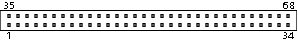 68 pin FEMALE connector at the peripherals |