Pinouts of Connectors

PC Card ATA connector pinout

layout
schematic diagram

add this page to bookmarks

This specification makes it possible to share ATA & PC Card with the same connectors.

68 pin MALE connector pin-out & layout
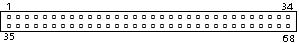
68 pin MALE connector  at the controller
Pin Namel Host Dir Dev PC-Card equiv
1 Ground x --> x Ground
2 DD3 x <-> x D3
3 DD4 x <-> x D4
4 DD5 x <-> x D5
5 DD6 x <-> x D6
6 DD7 x <-> x D7
7 /CS0 x --> x /CE1
8     --> i A10
9 /SELATA x --> x /OE
10          
11 /CS1 x --> x 1) A9
12     --> i A8
13          
14          
15     --> i /WE
16 INTRQ x <-- x /READY:IREQ
17 VCC x --> x VCC
18          
19          
20          
21          
22     --> i A7
23     --> i A6
24     --> i A5
25     --> i A4
26     --> i A3
27 DA2 x --> x A2
28 DA1 x --> x A1
29 DA0 x --> x A0
30 DD0 x <-> x D0
31 DD1 x <-> x D1
32 DD2 x <-> x D2
33 /IOCS16 x <-- x /WP:IOIS16
34 Ground x --> x Ground
35 Ground x --> x Ground
36 /CD1 x <-- x /CD1
37 DD11 x <-> x D11
38 DD12 x <-> x D12
39 DD13 x <-> x D13
40 DD14 x <-> x D14
41 DD15 x <-> x D15
42 /CS1 x --> x 1) /CE2
43     <-- i /VS1
44 /DIOR x --> x /IORD
45 /DIOW x --> x /IOWR
46          
47          
48          
49          
50          
51 VCC x --> x VCC
52          
53          
54          
55 M/S- x --> x 2)  
56 CSEL x --> x 2)  
57     <-- i /VS2
58 /RESET x --> x RESET
59 IORDY o <-- x 3) /WAIT
60 DMARQ o <-- x 3) /INPACK
61 /DMACK o --> o /REG
62 /DASP x <-> x /BVD2:SPKR
63 /PDIAG x <-> x /BVD1:STSCHG
64 DD8 x <-> x D8
65 DD9 x <-> x D9
66 DD10 x <-> x D10
67 /CD2 x <-- x /CD2
68 Ground x --> x Ground
x = Required.
i = Ignored by host in ATA mode.
o = Optional.
nothing = Not connected.
1) Device shall support only one /CS1 signal pin.
2) Device shall support either /M/S or CSEL but not both.
3) Device shall hold this signal negated if it does not support this function.

This information should be correct, but may be not. You can help us to improve this webpage!
You can confirm this document to be correct (be careful), or report an error in document (error may be described in the following webpage). Result of your submission will be used for calculating document status shown at the bottom of this page.
68 pin FEMALE connector pin-outs & layouts
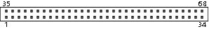
68 pin FEMALE connector  at the peripherals
Pinouts.ru > Pinouts of different motherboard slots >  Pinout of PC Card ATA connector and layout of 68 pin MALE connector and 68 pin FEMALE connector

Source(s): ATA-2 specifications, from Hardware Book
Document status: unknown
mark as erroneous!
mark as correct
0 report(s)
Click one of this links to change document status.
[Discuss at the forum] [Back to index] [Add new pinout]
[Report an error or update]
This information is maintained by pinouts.ru team and provided as a guideline only.
Efforts have been made to ensure it is correct, but it is the responsibility of the user
to verify the data is correct for their application.
80 hits since February 11, 2005