Pinouts of Connectors

30 pin SIMM connector pinout

layout
schematic diagram

add this page to bookmarks

SIMM=Single Inline Memory Module

30 pin SIMM connector pin-out & layout
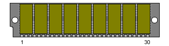
30 pin SIMM connector  at the computer
Pin Name Description
1 VCC +5 VDC
2 /CAS Column Address Strobe
3 DQ0 Data 0
4 A0 Address 0
5 A1 Address 1
6 DQ1 Data 1
7 A2 Address 2
8 A3 Address 3
9 GND Ground
10 DQ2 Data 2
11 A4 Address 4
12 A5 Address 5
13 DQ3 Data 3
14 A6 Address 6
15 A7 Address 7
16 DQ4 Data 4
17 A8 Address 8
18 A9 Address 9
19 A10 Address 10
20 DQ5 Data 5
21 /WE Write Enable
22 GND Ground
23 DQ6 Data 6
24 A11 Address 11
25 DQ7 Data 7
26 QP Data Parity Out
27 /RAS Row Address Strobe
28 /CASP Something Parity ????
29 DP Data Parity In
30 VCC +5 VDC

Note: SIMM above is a 4MBx9.
QP & DP is N/C on SIMMs without parity.
A9 is N/C on 256kB.
A10 is N/C on 256kB & 1MB. A11 is N/C on 256kB, 1MB & 4MB.

This information should be correct, but may be not. You can help us to improve this webpage!
You can confirm this document to be correct (be careful), or report an error in document (error may be described in the following webpage). Result of your submission will be used for calculating document status shown at the bottom of this page.
Pinouts.ru > Pinouts of different memory connectors >  Pinout of 30 pin SIMM connector and layout of 30 pin SIMM connector

Source(s):  comp.sys.ibm.pc.hardware.* FAQ Part 4, maintained by Ralph Valentino, from J. Ogren and Helfried Behre, comp.sys.ibm.pc.hardware.* FAQ Part 4, maintained by Ralph Valentino
Document status: unknown
mark as erroneous!
mark as correct
0 report(s)
Click one of this links to change document status.
[Discuss at the forum] [Back to index] [Add new pinout]
[Report an error or update]
This information is maintained by pinouts.ru team and provided as a guideline only.
Efforts have been made to ensure it is correct, but it is the responsibility of the user
to verify the data is correct for their application.
83 hits since February 12, 2005