Pinouts of Connectors

VESA Feature connector pinout

layout
schematic diagram

add this page to bookmarks

26 pin IDC MALE connector pin-out & layout
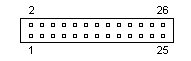
26 pin IDC MALE connector  at the Video card
Pin Name Description
1 PD0 DAC Pixel Data Bit 0 (PB)
2 PD1 DAC Pixel Data Bit 1 (PG)
3 PD2 DAC Pixel Data Bit 2 (PR)
4 PD3 DAC Pixel Data Bit 3 (PI)
5 PD4 DAC Pixel Data Bit 4 (SB)
6 PD5 DAC Pixel Data Bit 5 (SG)
7 PD6 DAC Pixel Data Bit 6 (SR)
8 PD7 DAC Pixel Data Bit 7 (SI)
9 CLK DAC Clock
10 BLK DAC Blanking
11 HSYNC Horizontal Sync
12 VSYNC Vertical Sync
13 GND Ground
14 GND Ground
15 GND Ground
16 GND Ground
17   Select Internal Video
18   Select Internal Sync
19   Select Internal Dot Clock
20 n/c Not used
21 GND Ground
22 GND Ground
23 GND Ground
24 GND Ground
25 n/c Not used
26 n/c Not used

Pinouts.ru > Pinouts of video connectors >  Pinout of VESA Feature connector and layout of 26 pin IDC MALE connector

Source(s): Hardware Book
Document status: correct
mark as erroneous!
mark as correct
1 report(s)
Click one of this links to change document status.
[Discuss at the forum] [Back to index] [Add new pinout]
[Report an error or update]
This information is maintained by pinouts.ru team and provided as a guideline only.
Efforts have been made to ensure it is correct, but it is the responsibility of the user
to verify the data is correct for their application.
120 hits since February 11, 2005