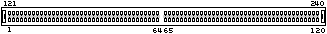
 240 pin DIMM DDR2 connector at the motheboard |
| Pin # |
Description |
Pin # |
Description |
| 1 |
VREF |
121 |
VSS |
| 2 |
VSS |
122 |
DQ4 |
| 3 |
DQ0 |
123 |
DQ5 |
| 4 |
DQ1 |
124 |
VSS |
| 5 |
VSS |
125 |
DM0 |
| 6 |
/DQS0 |
126 |
NC |
| 7 |
DQS0 |
127 |
VSS |
| 8 |
VSS |
128 |
DQ6 |
| 9 |
DQ2 |
129 |
DQ7 |
| 10 |
DQ3 |
130 |
VSS |
| 11 |
VSS |
131 |
DQ12 |
| 12 |
DQ8 |
132 |
DQ13 |
| 13 |
DQ9 |
133 |
VSS |
| 14 |
VSS |
134 |
DM1 |
| 15 |
/DQS1 |
135 |
NC |
| 16 |
DQS1 |
136 |
VSS |
| 17 |
VSS |
137 |
CK1 |
| 18 |
NC |
138 |
/CK1 |
| 19 |
NC |
139 |
VSS |
| 20 |
VSS |
140 |
DQ14 |
| 21 |
DQ10 |
141 |
DQ15 |
| 22 |
DQ11 |
142 |
VSS |
| 23 |
VSS |
143 |
DQ20 |
| 24 |
DQ16 |
144 |
DQ21 |
| 25 |
DQ17 |
145 |
VSS |
| 26 |
VSS |
146 |
DM2 |
| 27 |
/DQS2 |
147 |
NC |
| 28 |
DQS2 |
148 |
VSS |
| 29 |
VSS |
149 |
DQ22 |
| 30 |
DQ18 |
150 |
DQ23 |
| 31 |
DQ129 |
151 |
VSS |
| 32 |
VSS |
152 |
DQ28 |
| 33 |
DQ24 |
153 |
DQ29 |
| 34 |
DQ25 |
154 |
VSS |
| 35 |
VSS |
155 |
DM3 |
| 36 |
/DQS3 |
156 |
NC |
| 37 |
DQS3 |
157 |
VSS |
| 38 |
VSS |
158 |
DQ30 |
| 39 |
DQ26 |
159 |
DQ31 |
| 40 |
DQ27 |
160 |
VSS |
| 41 |
VSS |
161 |
NC |
| 42 |
NC |
162 |
NC |
| 43 |
NC |
163 |
VSS |
| 44 |
VSS |
164 |
NC |
| 45 |
NC |
165 |
NC |
| 46 |
NC |
166 |
VSS |
| 47 |
VSS |
167 |
NC |
| 48 |
NC |
168 |
NC |
| 49 |
NC |
169 |
VSS |
| 50 |
VSS |
170 |
VDDQ |
| 51 |
VDDQ |
171 |
CK1 |
| 52 |
CKE0 |
172 |
VDD |
| 53 |
VDD |
173 |
NC |
| 54 |
NC |
174 |
NC |
| 55 |
NC |
175 |
VDDQ |
| 56 |
VDDQ |
176 |
A12 |
| 57 |
A11 |
177 |
A9 |
| 58 |
A7 |
178 |
VDD |
| 59 |
VDD |
179 |
A8 |
| 60 |
A5 |
180 |
A6 |
| 61 |
A4 |
181 |
VDDQ |
| 62 |
VDDQ |
182 |
A3 |
| 63 |
A2 |
183 |
A1 |
| 64 |
VDD |
184 |
VDD |
| KEY |
| 65 |
VSS |
185 |
CK0 |
| 66 |
VSS |
186 |
/CK0 |
| 67 |
VDD |
187 |
VDD |
| 68 |
NC |
188 |
A0 |
| 69 |
VDD |
189 |
VDD |
| 70 |
A10/AP |
190 |
BA1 |
| 71 |
BA0 |
191 |
VDDQ |
| 72 |
VDDQ |
192 |
/RAS |
| 73 |
/WE |
193 |
/CS0 |
| 74 |
/CAS |
194 |
VDDQ |
| 75 |
VDDQ |
195 |
ODT0 |
| 76 |
/CS1 |
196 |
A13 |
| 77 |
ODT1 |
197 |
VDD |
| 78 |
VDDQ |
198 |
VSS |
| 79 |
VSS |
199 |
DQ36 |
| 80 |
DQ32 |
200 |
DQ37 |
| 81 |
DQ33 |
201 |
VSS |
| 82 |
VSS |
202 |
DM4 |
| 83 |
/DQS4 |
203 |
NC |
| 84 |
DQS4 |
204 |
VSS |
| 85 |
VSS |
205 |
DQ38 |
| 86 |
DQ34 |
206 |
DQ39 |
| 87 |
DQ35 |
207 |
VSS |
| 88 |
VSS |
208 |
DQ44 |
| 89 |
DQ40 |
209 |
DQ45 |
| 90 |
DQ41 |
210 |
VSS |
| 91 |
VSS |
211 |
DM5 |
| 92 |
/DQS5 |
212 |
NC |
| 93 |
DQS5 |
213 |
VSS |
| 94 |
VSS |
214 |
DQ46 |
| 95 |
DQ42 |
215 |
DQ47 |
| 96 |
DQ43 |
216 |
VSS |
| 97 |
VSS |
217 |
DQ52 |
| 98 |
DQ48 |
218 |
DQ53 |
| 99 |
DQ49 |
219 |
VSS |
| 100 |
VSS |
220 |
CK2 |
| 101 |
SA2 |
221 |
/CK2 |
| 102 |
NC |
222 |
VSS |
| 103 |
VSS |
223 |
DM6 |
| 104 |
/DQS6 |
224 |
NC |
| 105 |
DQS6 |
225 |
VSS |
| 106 |
VSS |
226 |
DQ54 |
| 107 |
DQ50 |
227 |
DQ55 |
| 108 |
DQ51 |
228 |
VSS |
| 109 |
VSS |
229 |
DQ60 |
| 110 |
DQ56 |
230 |
DQ61 |
| 111 |
DQ57 |
231 |
VSS |
| 112 |
VSS |
232 |
DM7 |
| 113 |
/DQS7 |
233 |
NC |
| 114 |
DQS7 |
234 |
VSS |
| 115 |
VSS |
235 |
DQ62 |
| 116 |
DQ58 |
236 |
DQ63 |
| 117 |
DQ59 |
237 |
VSS |
| 118 |
VSS |
238 |
VDDSPD |
| 119 |
SDA |
239 |
SA0 |
| 120 |
SCL |
240 |
SA1 |
Some pins functions:
A0 to A13 Address input
BA0, BA1 Bank select address
DQ0 to DQ63 Data input/output
/RAS Row address strobe command
/CAS Column address strobe command
/WE Write enable
/CS0, /CS1 Chip select
CKE0, CKE1 Clock enable
CK0 to CK2 Clock input
/CK0 to /CK2 Differential clock input
DQS0 to DQS7, /DQS0 to /DQS7
Input and output data strobe
DM0 to DM7 Input mask
SCL Clock input for SPD
SDA Data input/output for SPD
SA0 to SA2 Serial address input
VDD Power for internal circuit
VDDQ Power for DQ circuit
VDDSPD Power for serial EEPROM
VREF Input reference voltage
VSS Ground
ODT0, ODT1 ODT control
NC No Connection
This information should be correct, but may be not. You can help us to improve this webpage!
You can confirm this document to be correct (be careful), or report an error in document (error may be described in the following webpage). Result of your submission will be used for calculating document status shown at the bottom of this page. |
| |