Pinouts of Connectors

EIA-449 (RS-449) interface pinout

layout
schematic diagram

add this page to bookmarks

The RS449 interface is a generic connector specification. It´s not an actual interface. The connector pinning was originally designed to support RS422 for balanced signals, and RS423 for the unbalanced signals. And should have been the succesor of RS232.

37 pin D-SUB MALE connector pin-out & layout
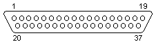
37 pin D-SUB MALE connector  at the DTE (Computer)

RS449 is a high speed digital interface - unlike RS232 which uses signals with reference to ground, RS449 V.11 receivers look for the difference between two wires. By twisting the two wires and making a "twisted pair" any stray noise picked up on one wire will be picked up on the other, because both wires pick up the same noise the RS449 differential interface just shifts in voltage level with reference to ground, but does not change with respect to each other. The receivers are only looking at the difference in voltage level of each wire to the other not to ground.

The differential signals for RS449 are labeled as either "A and B" or "+ and -". In the case of RS449 wire A or + does not connect to B or -. Wire A always connects to A and B connects to B or + to + and - to -. If you do cross the wires you just inverted the data or clock in your interface and they don"t work - be sure to check the polarities .

Common names: EIA-449, RS-449, ISO 4902.

Primary channel

Pin Name V.24 Dir Description Type
1   101 --- Shield Ground
2 SI 112 --> Signal Rate Indicator Control
3 n/a   n/a unused  
4 SD- 103 --> Send Data (A) Data
5 ST- 114 <-- Send Timing (A) Timing
6 RD- 104 <-- Receive Data (A) Data
7 RS- 105 --> Request To Send (A) Control
8 RT- 115 <-- Receive Timing (A) Timing
9 CS- 106 <-- Clear To Send (A) Control
10 LL 141 --> Local Loopback Control
11 DM- 107 <-- Data Mode (A) Control
12 TR- 108.2 --> Terminal Ready (A) Control
13 RR- 109 <-- Receiver Ready (A) Control
14 RL 140 --> Remote Loopback Control
15 IC 125 <-- Incoming Call Control
16 SF/SR+ 126 <-> Signal Freq./Sig. Rate Select. Control
17 TT- 113 --> Terminal Timing (A) Timing
18 TM- 142 <-- Test Mode (A) Control
19 SG 102 --- Signal Ground Ground
20 RC 102b --- Receive Common Ground
21 n/a   n/a unused  
22 SD+ 103 --> Send Data (B) Data
23 ST+ 114 <-- Send Timing (B) Timing
24 RD+ 104 <-- Receive Data (B) Data
25 RS+ 105 --> Request To Send (B) Control
26 RT+ 115 <-- Receive Timing (B) Timing
27 CS+ 106 <-- Clear To Send (B) Control
28 IS n/a --> Terminal In Service Control
29 DM+ 107 <-- Data Mode (B) Control
30 TR+ 108.2 --> Terminal Ready (B) Control
31 RR+ 109 <-- Receiver Ready (B) Control
32 SS 116 <-- Select Standby Control
33 SQ 110 <-- Signal Quality Control
34 NS n/a --> New Signal Control
35 TT+ 113 --> Terminal Timing (B) Timing
36 SB 117 <-- Standby Indicator Control
37 SC 102a --- Send Common Ground

Note: Direction is DTE (Computer) relative DCE (Modem).

Name Description Function
AA Shield Ground Also known as protective ground. This is the chassis ground connection between DTE and DCE.
AB Signal Ground The reference ground between a DTE and a DCE. Has the value 0 Vdc.
BA Transmitted Data Data send by the DTE.
BB Received Data Data received by the DTE.
CA Request To Send Originated by the DTE to initiate transmission by the DCE.
CB Clear To Send Send by the DCE as a reply on the RTS after a delay in ms, which gives the DCEs enough time to energize their circuits and synchronize on basic modulation patterns.
CC DCE Ready Known as DSR. Originated by the DCE indicating that it is basically operating (power on, and in functional mode).
CD DTE Ready Known as DTR. Originated by the DTE to instruct the DCE to setup a connection. Actually it means that the DTE is up and running and ready to communicate.
CE Ring Indicator A signal from the DCE to the DTE that there is an incomming call (telephone is ringing). Only used on switched circuit connections.
CF Received Line Signal Detector Known as DCD. A signal send from DCE to its DTE to indicate that it has received a basic carrier signal from a (remote) DCE.
CH/CI Data Signal Rate Select
(DTE/DCE Source>
A control signal that can be used to change the transmission speed.
DA Transmit Signal Element Timing
(DTE Source)
Timing signals used by the DTE for transmission, where the clock is originated by the DTE and the DCE is the slave.
DB Transmitter Signal Element Timing
(DCE Source)
Timing signals used by the DTE for transmission.
DD Receiver Signal Element Timing
(DCE Source)
Timing signals used by the DTE when receiving data.
IS terminal In Service Signal that indicates that the DTE is available for operation
NS New Signal A control signal from the DTE to the DCE. It instructs the DCE to rapidly get ready to receive a new analog signal. It helps master-station modems rapidly synchronize on a new modem at a tributary station in multipoint circuits
RC Receive Common A signal return for receiver circuit reference
LL Local Loopback / Quality Detector A control signal from the DTE to the DCE that causes the analog transmision output to be connected to the analog receiver input.
RL Remote Loopback Signal from the DTE to the DCE. The local DCE then signals the remote DCE to loopback the analog signal and thus causing a line loopback.
SB Standby Indicator Signal from the DCE to indicate if it is uses the normal communication or standby channel
SC Send Common A return signal for transmitter circuit reference
SF Select Frequency A signal from the DTE to tell the DCE which of the two analog carrier frequencies should be used.
SS Select Standby A signal from DTE to DCE, to switch between normal communication or standby channel.
TM Test Mode A signal from the DCE to the DTE that it is in test-mode and can"t send any data.
  Reserved for Testing  

The EIA RS449 standard specifies the functional and mechanical characteristics of the RS449 interconnection between the data terminal equipment (DTE) in the data communications equipment (DCE) complying to EIA electrical interface standards RS 422 and RS 423.

This information should be correct, but may be not. You can help us to improve this webpage!
You can confirm this document to be correct (be careful), or report an error in document (error may be described in the following webpage). Result of your submission will be used for calculating document status shown at the bottom of this page.
37 pin D-SUB FEMALE connector pin-outs & layouts
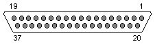
37 pin D-SUB FEMALE connector  at the DCE (Modem)
Pinouts.ru > Pinouts of serial ports >  Pinout of EIA-449 (RS-449) interface and layout of 37 pin D-SUB MALE connector and 37 pin D-SUB FEMALE connector

Source(s): RS449 Page at Connectivity Knowledge Platform (Made IT), arcelect.com
Document status: unknown
mark as erroneous!
mark as correct
0 report(s)
Click one of this links to change document status.
[Discuss at the forum] [Back to index] [Add new pinout]
[Report an error or update]
This information is maintained by pinouts.ru team and provided as a guideline only.
Efforts have been made to ensure it is correct, but it is the responsibility of the user
to verify the data is correct for their application.
86 hits since February 12, 2005