VMEbus connector pinout |
layout |
VMEbus is a computer bus standard originally developed for the Motorola 68000 line of CPUs, but later widely used for many applications.
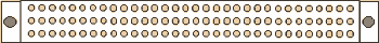 96 pin DIN 41612 (3x32) FEMALE connector at the backplane | VMEBus is physically based on the Eurocard sizes, mechanicals and connectors, but uses its own signalling system, which Eurocard does not define. It was first developed in 1981, and continues to see widespread use today. In many ways the VMEbus is the pins of the 68000 run out onto a backplane. In most cases this is a bad design, because it limits you to systems similar to the chipset the bus was originally designed for. (For instance, the ISA bus is still useful only for Intel chips). However one of the key features of the 68000 was a flat 32-bit memory model, free of memory segmentation and other "anti-features". The result is that while VME is very 68000-like, the 68000 is generic enough to make this a non-issue in most cases. Like the 68000, VME uses separate data and address buses, both 32-bits. In the case of the 68000 the address bus was actually 24-bits and the data bus 16-bits (although it was 32/32 internally), but the designers were already looking towards full 32-bit implementations. In order to allow both widths of buses to be used, VME uses two different Eurocard connectors, the P1 and P2. P1 contains three rows of 32 pins each, implementing the first 24-bits of the address and 16-bits of the data buses, along with all of the control signals. The P2 contains one more row, which includes the remaining 8 address and 16 data pins. In order to control the bus a set of nine lines known as the arbitration bus is used. All communications are controlled by the card inserted in slot one of the Eurocard chassis, known as the arbiter module. In general use the cards will request access to the bus by holding the bus request in lines of the arbitration bus low to indicate their slot number. When the arbiter module frees the bus it scans these lines to see if there are any held low. If so, it pulls the bus busy line low to indicate the bus is going busy again, and writes the card number back out on the bus grant out lines. At this point the numbered card has gained access to the bus. To write data the card writes the address and data to the bus, and then pulls the address strobe line and the two data strobe lines low to indicate the data is ready, and then pulls the write pin to indicate the operation. There are two data strobes so the cards can indicate if the data is 8, 16, or 32 bits (or 64 in VME64). The card at the indicated address on the bus then reads the data and pulls the data transfer acknowledge line when it is complete (or the bus error line if need be). Reading data is essentially the same, but the controlling card places only the address on the bus and pulls the READ pin. The other card then writes the data and pulls the data strobe pins when the data is ready. This signalling scheme is asynchronous, meaning that there is no overall clock signal as there is in synchronous buses such as PCI. VME also includes an interrupt bus, supplying all seven of the 68000"s interrupt pins. When an interrupt is supplied the arbiter module writes the interrupt level back out to the address bus to tell which interrupt is being handled. Note that there is no concept of card number in this case, because cards will often share interrupts. The excessive number of interrupt levels has often been pointed to as one of the few examples of overdesign in the 68000, and it makes even less sense in the case of a bus. Note that in VME all transfers are DMA and every card is a master (or slave). In most bus standards there is a considerable amount of complexity added in order to support various transfer types and master/slave selection. For instance, in the ISA bus both of these features had to be added on top of the already existing "channels" model where all communications was handled by the host CPU. This makes VME considerably simpler at a conceptual level while being more powerful, although it requires somewhat more complex controllers on each card in order to work. J=Jack (Backplane), P=Plug (Board) P1/J1 (Required)
P2/J2 (Optional)
*) Active Low
| ||||||||||||||||||||||||||||||||||||||||||||||||||||||||||||||||||||||||||||||||||||||||||||||||||||||||||||||||||||||||||||||||||||||||||||||||||||||||||||||||||||||||||||||||||||||||||||||||||||||||||||||||||||||||||||||||||||||||||||||||||||||||||||||||||||||||||
Pinouts.ru > Pinouts of different motherboard slots > Pinout of VMEbus connector and layout of 96 pin DIN 41612 (3x32) FEMALE connector Source(s): VMEbus connector Pin Assignment at VITA"s VMEbus FAQcomp.arch.bus.vmebus FAQ by Robert J. Boys, wikipedia.org VMEbus, from Hardware Book, Kevin D. Plymel, and many more | unknown | |
|
mark as correct |
0 report(s) | |
| Click one of this links to change document status. | ||