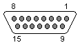
 15 pin D-SUB FEMALE connector at the DTE (Computer) | CCITT X21 is a physical and electrical interface that uses two types of circuits:
balanced (X.27N.1 1) and and unbalanced (X.26N.10). CCITT X.21 calls out the DB-15 connector.
The physical interface between the DTE and the local PTT-supplied DCE is defined in ITU-T recommendation X.21. The DCE provides a full-duplex, bit-serial, synchronous transmission path between the DTE and the local PSE. It can operate at data rates from 600bps to 64Kbps. A second standard, X.21bis has been defined for use on existing (analogue) networks. An X.21bis is a subset of EIA-232D/V.24 therefore allowing existing user equipment to be readily interfaced using this standard. It should perhaps be emphasized here that V24 defines the data terminal equipment interface to the modem and is not concerned with the interface between the modem and the line itself. The modems themselves therefore form part of the conceptual physical connection. The V24 interface is thus independent of both modulation technique and data throughput rate.
| Pin |
Name |
Dir |
Description |
Type |
| 1 |
n/a |
 |
Shield |
Ground |
| 2 |
T (A) |
 |
Transmit (A) |
Data |
| 3 |
C (A) |
|
Control (A) |
Control |
| 4 |
R (A) |
 |
Receive (A) |
Data |
| 5 |
I (A) |
|
Indication (A) |
Control |
| 6 |
S (A) |
|
Signal Timing (A) |
Timing |
| 7 |
B (A) |
|
Byte Timing (A) |
Timing |
| 8 |
G |
|
Ground |
Ground |
| 9 |
T (B) |
|
Transmit (B) |
Data |
| 10 |
C (B) |
|
Control (B) |
Control |
| 11 |
R (B) |
|
Receive (B) |
Data |
| 12 |
I (B) |
|
Indication (B) |
Control |
| 13 |
S (B) |
|
Signal Timing (B) |
Timing |
| 14 |
B (B) |
|
Byte Timing (B) |
Timing |
| 15 |
|
|
unused |
|
All signals are balanced. Meaning there is always a pair (+/-) for each signal, like used in RS422. Electrally the X.21 signals are the same as RS422, so please refer to RS422 for the exact details.
As can be seen from the pinning specifications, the Signal Element Timing (clock) is provided by the DCE. This means that your provider (local telco office) is responisble for the correct clocking and that X.21 is a synchronous interface. Hardware handshaking is done by the Control and Indication lines. The Control is used by the DTE and the Indication is the DCE one.
Description of signals:
| Signal Ground (G) - |
This provides reference for the logic states against the other circuits.
This signal may be connected to the protective ground (earth). |
| DTE Common Return (Ga) - |
Used only in unbalanced-type configurations (X.26), this signal provides
reference ground for receivers in the DCE interface. |
| Transmit (T) - |
This carries the binary signals which carry data from the DTE to the
DCE. This circuit can be used in data-transfer phases or in call-control
phases from the DTE to DCE (during Call Connect or Call Disconnect). |
| Receive (R) - |
Controlled by the DTE to indicate to the DCE the meaning of the data
sent on the transmit circuit. This circuit must be ON during data-transfer
phase and can be ON or OFF during call-control phases, as defined by the
protocol. |
| Indication (I) - |
The DCE controls this circuit to indicate to the DTE the type of data
sent on the Receive line. During data phase, this circuit must be ON and
it can be ON or OFF during call control, as defined by the protocol. |
| Signal Element Timing (S) - |
This provides the DTE or DCE with timing information for sampling the
Receive line or Transmit line. The DTE samples at the correct instant to
determine if a binary 1 or 0 is being sent by the DCE. The DCE samples to
accurately recover signals at the correct instant. This signal is always
ON. |
| Byte Timing (B) - |
This circuit is normally ON and provides the DTE with 8-bit byte element
timing. The circuit transitions to OFF when the Signal Element Timing circuit
samples the last bit of an 8-bit byte. Call-control characters must align
with the B lead during call-control phases. During data- transfer phase,
the communicating devices bilaterally agree to use the B lead to define
the end of each transmitted or received byte. The C and I leads then only
monitor and record changes in this condition when the B lead changes from
OFF to ON, although the C and I leads may be altered by the transitions
on the S lead. This lead is frequently not used. |
Note: Direction is DTE (Computer) relative DCE (Modem) This information should be correct, but may be not. You can help us to improve this webpage!
You can confirm this document to be correct (be careful), or report an error in document (error may be described in the following webpage). Result of your submission will be used for calculating document status shown at the bottom of this page. |
| 15 pin D-SUB FEMALE connector at the DCE (Modem) |